Advantages of low power DC/DC converters
After more than fifty years of historical development, the complexity of converting DC voltage into another DC voltage display in electronic circuits has continued to increase, and modern designs have incredibly high power density while increasing efficiency to maintain small power. RECOM has many innovative designs that apply high-power supply design techniques to low-power converters in small packages.
The first DC/DC conversion solutions are all low-noise linear designs that are easy to use but have two major drawbacks. First, the output voltage must be lower than the input voltage; Linear regulators are very inefficient and dissipate most of the power provided in the form of heat. Second, depending on the voltage difference between the input and output, the efficiency of a linear regulator may be only 60% or less.
The invention of the DC/DC switching converter solved both problems, but required a more complex design approach. In contrast to linear designs, switching converters take advantage of the energy storage characteristics of inductive and capacitor components to transmit power in discrete device packages. The power pulse is stored in the inductor's magnetic field or the capacitor's electric field.
The switching controller ensures that only the power required by the load is transmitted per switching cycle, so the topology is highly efficient. Good designcan achieve efficiency of 97% or more. A simplified block diagram of a switching DC/DC converter is shown in Figure 1.
Figure 1: Simplified block diagram of switching regulator
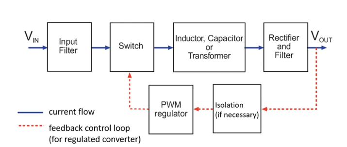
The switching function in Figure 1 is performed by the power transistor, which alternates between efficient "on" and "off" states in a controlled sequence. This is in contrast to continuous operation in linear design. DC/DC switching converters can produce an output higher or lower than the input (boost or buck) or reverse the input voltage to the output.
The output can be regulated or unregulated. The output voltage of an unregulated converter varies with the load current or input voltage. If the voltage is regulated, the feedback control loop (dotted line) feeds the output voltage back to the switch block; This alters the switching operation to compensate for output voltage deviations, whether these are caused by input voltage changes (such as slow battery depletion) or load changes.
The simplest switching topology shares a common ground current path between the input and output and is therefore non-isolated, where the inductive component is the inductor. The isolation converter has a current isolation between the input and output, and transmits power through the electromagnetic field generated by the transformer coupling windings. Since the output is isolated from the input, it does not matter whether the input voltage is of the same polarity as the output voltage. In a linear design, the ground return current flows directly between input and output, so it cannot be isolated, and only three pins are required: Vin, common ground, and Vout.
Low power DC/DC converter topology
Better performance goes hand in hand with higher cost, more complexity, and a larger footprint, which is almost a fact of power supply design. Small DC/DC converter users value package and cost performance, so how can RECOM meet their requirements for low-power isolated DC/DC products?
Push-pull topologies are widely used to isolate DC/DC converters. This is a low-cost way to generate higher, lower, or inverting voltages because the transformer turns ratio determines the output voltage. The topology is simple, the efficiency is reasonable and the electromagnetic radiation is relatively low.
Figure 2: Push-pull DC/DC converter with unregulated output
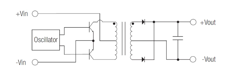
Figure 2 shows a block diagram of a push-pull isolated DC/DC converter with unregulated output. To save space, the oscillator and drive transistor can be combined in a dedicated push-pull transformer driver IC.
For a regulated output, the simplest method is to add a linear regulator in series with the +Vout line on the secondary side, as shown in Figure 3. This method can achieve the desired goal, but also suitable for the design of very low power DC/DC. The RECOM RY/P series, for example, offers short circuit protection and low noise voltage regulator output.
Figure 3: Push-pull DC/DC converter with regulated output
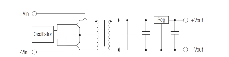
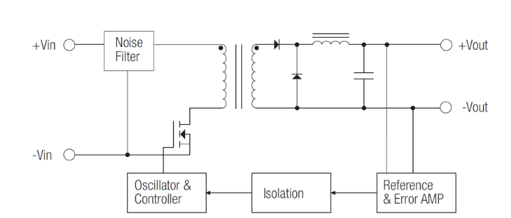
This type of design can achieve about 65-75% efficiency. Maximizing efficiency when the power is greater than 1W or 2W is the primary task, and the design needs to be further improved, so it is necessary to switch from secondary side regulation to primary side regulation. In place of a linear regulator, the output voltage is monitored on the secondary side and compared to the target voltage to generate a voltage difference, which is then sent back to the primary side oscillator controller. This adjusts the switching frequency to zero out the error.
Since this is an isolated design, the error signal must also be isolated. Figure 4 shows RECOM's voltage regulator converters above rated power of 3W using this method, which can increase the efficiency to about 85%.
Figure 4: The secondary side error signal provides feedback to the primary side controller
DC/DC converters with higher output power require more complex methods to handle. Not only does the linear regulator waste power in the above way, but the two secondary side diodes are also the cause of loss. The forward voltage drop of a power diode is usually 0.5V, which means that the 1A has a power loss of 0.5W.
The solution is a synchronous rectifier consisting of two FET Fets and a controller instead of a diode and linear regulator.
Figure 5: Passive rectification (left) and synchronous rectification (right)

Figure 5 compares the two approaches. The FET is turned on on the forward part of the cycle and turned off on the reverse part of the cycle to act as a rectifier. The combination of fast switching and very low on-resistance RDS(ON) of about 10 Mω makes the FET ideal for rectifiers. The disadvantage is that they must be driven actively, so additional timing and drive circuits are required to detect the internal voltage and properly turn the two FETs on and off to synchronize with the output waveform. Diodes are passive devices that do not require additional circuitry to operate, but the higher efficiency of synchronous rectification more than offsets the increased cost complexity of pursuing high output current converters.
Figure 6: The RP20 uses a variety of design techniques to improve efficiency
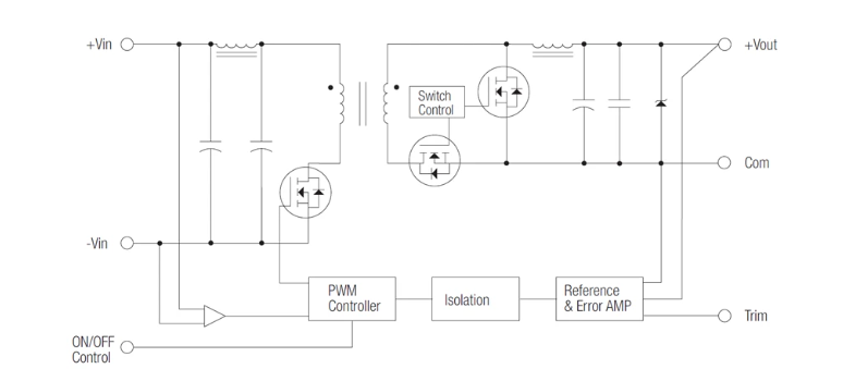
RECOM's RP20 Series 20W DC/DC converters use synchronous rectifiers with up to 89% efficiency. The design also includes the isolated error signal described above. Finally, the RP20 in Figure 6 achieves 85-89% efficiency over a wide load range.
Conclusion
The design idea of high-power power supply is borrowed from the DC/DC converter with minimal power to achieve higher efficiency. As our customers' demands for power levels increased, we had to make appropriate changes to change the priority of demand. RECOM is the industry leader in delivering the best combination of cost advantage and package size design.
Heisener Electronic is a famous international One Stop Purchasing Service Provider of Electronic Components. Based on the concept of Customer-orientation and Innovation, a good process control system, professional management team, advanced inventory management technology, we can provide one-stop electronic component supporting services that Heisener is the preferred partner for all the enterprises and research institutions.