In order to meet the demand of the market for miniaturization and energy efficiency, Infineon Technology Co., Ltd. has launched a new CoolMOS PFD7 high-voltage MOSFET series, setting a new industry standard for 950V superjunction (SJ) technology. The new 950V series has excellent performance and ease of use. The integrated fast body diode ensures the robustness of the device, while reducing the BOM (bill of materials) cost. This product is specially designed for ultra-high power density and ultra-high efficiency products, and is mainly used for lighting systems and switching power supply (SMPS) applications in consumer and industrial fields.
The new product line is suitable for flyback, PFC and LLC/LCC designs, including half bridge or full bridge configurations that make power commutation stable and reliable. By integrating ultrafast body diode with ultra-low reverse recovery charge (Qrr), this series of products realizes the robustness and reliability of hard commutation, and becomes a more robust super junction MOSFET in this voltage level, which can be applied to all topologies in the target application. In addition, the substantial reduction of switching losses (EOSS, QOSS and Qg) also improves the efficiency of hard switching and soft switching applications. Compared with 900V CoolMOS C3 superjunction MOSFET, the MOSFET temperature can be reduced by up to 4 Kelvin. Compared with the previous products, the new products are more green and environmentally friendly, and their light load and full load PFC efficiency has been improved by more than 0.2%, while meeting the efficiency requirements of LLCs.
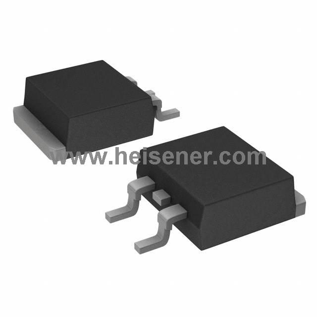
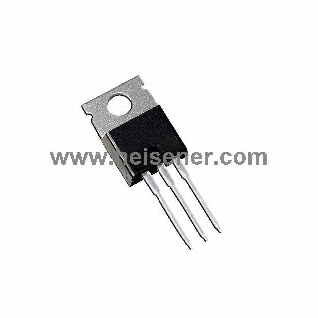
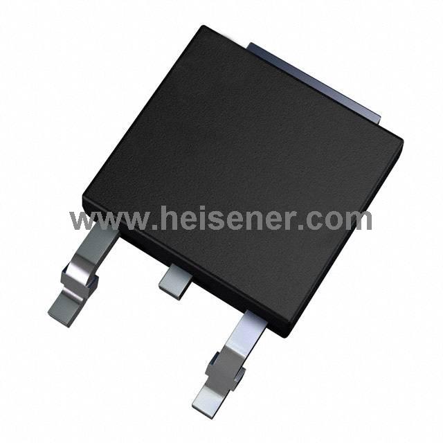
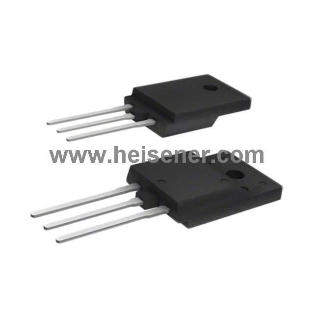
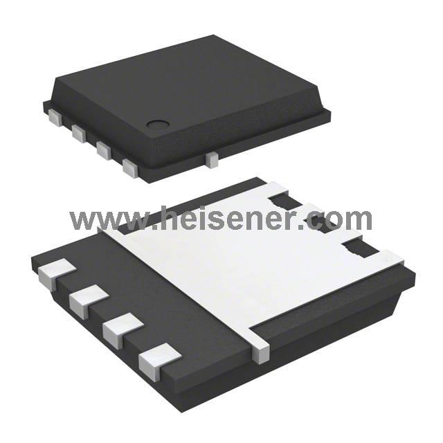
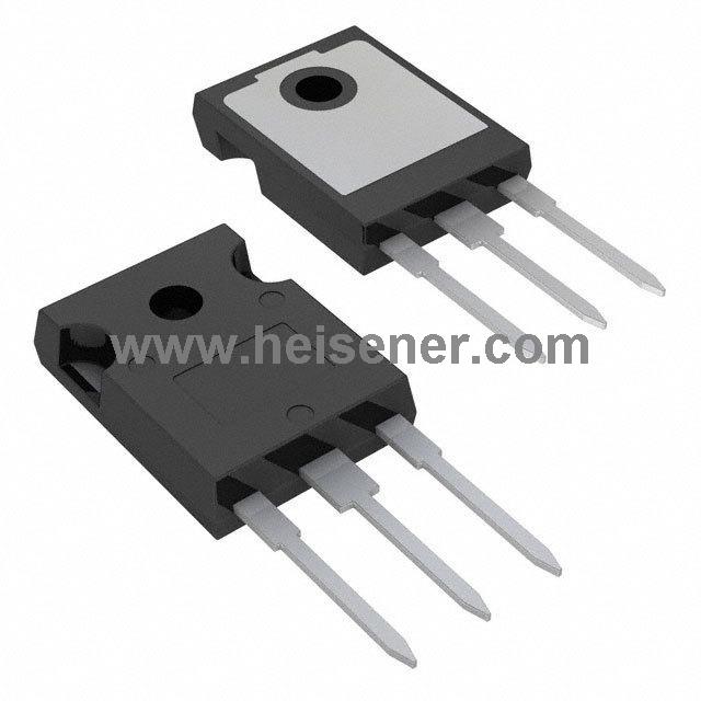
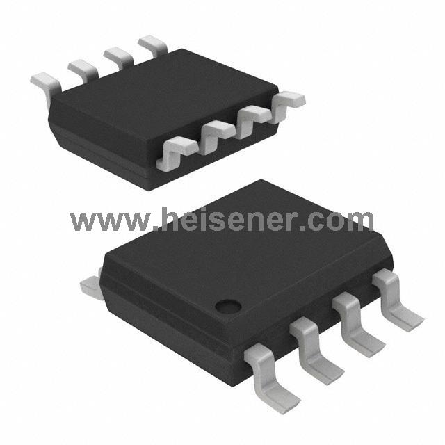
The new product series has reduced the on resistance (RDS (on)) value of various SMD and THD packaged devices by up to 55%. For example, the on resistance value of devices in DPAK package is 450 m Ω or the on resistance value of devices in TO247 package is 60 m Ω. Designers can reduce BOM cost and production cost by reducing package size, greatly increasing power density and saving circuit board space. Its gate source threshold voltage (V (GS), th) is 3V, V (GS), and the minimum variation range of th is ± 0.5V, which facilitates the design import and drive of new devices and improves the design freedom; The use of low threshold voltage and tolerance can avoid the use of MOSFET linear mode and reduce the drive voltage and idle loss. In addition, compared with CoolMOS C3, the grid charge of the new product series has been improved by 60%, greatly reducing the drive loss, and can reach the Human Body Discharge Model (HBM) (Level 2 Electrostatic Discharge Sensitivity) standard, ensuring the robustness of electrostatic discharge (ESD), thereby reducing ESD related equipment failures and increasing the output.